
Custom Physical Design Services for ASIC & SoC Development
Flat No 212, Plot No. 32 to 34 & 39 to 41, KTC ILLUMINATION, GAFOOR NAGAR , Hyderabad, Telangana
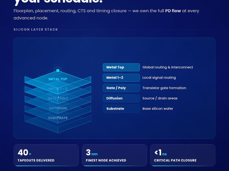
Silicon Patterns provides end-to-end Physical Design services for ASIC and SoC development, helping semiconductor companies achieve high-performance, manufacturable silicon. Our experienced engineering team handles the complete backend implementation flow, including floorplanning, power planning, placement, clock tree synthesis (CTS), routing, timing closure, physical verification, and GDSII signoff.
With expertise across advanced technology nodes from 28nm to 3nm and experience supporting 40+ successful tapeouts, we deliver optimized designs with a strong focus on timing, power, area, and reliability. Whether you require complete physical implementation or support for a specific stage of the design flow, our team works closely with you to accelerate tapeout while minimizing design risk.
Contact us to discuss your next ASIC or SoC project.
sales@siliconpatterns.com
http://www.siliconpatterns.com